

Controlling Trace Contamination In Semiconductor Fluid Networks To Improve Wafer Yield
May 28, 2026
Leave a message
Yield engineering in a modern semiconductor fab is largely an exercise in particle management. As transistor geometries shrink toward sub-three-nanometer thresholds, traditional macro-level contaminants are no longer the only threat. Microscopic variations in chemical purity, minor pressure fluctuations, and trace metallic ions in the process stream now directly cause catastrophic chip failures.
While tool parameters like plasma density and laser focus get most of the attention, the physical infrastructure delivering chemicals, solvents, and ultra-pure water to the wet bench is often where yield loss actually happens.

Semiconductor
Process Defect Classification and Liquid-Phase Root Causes
Defects found during inline inspection are generally classified as either intrinsic material anomalies or process-induced surface contamination. Lattice defects, including vacancies and dislocations, usually trace back to the initial ingot growth. On the other hand, bridging shorts, patterned crystal defects, and gate oxide breakdown are almost always introduced during lithography, stripping, etching, or chemical mechanical planarization.
During these wet chemistry steps, the silicon wafer surface is highly reactive and vulnerable to any foreign matter suspended in the process chemicals. If a delivery line introduces sub-micron particulates, these grains lodge between fine metal lines during deposition, creating an immediate electrical short.
Chemical contamination is even more insidious. Heavy metal ions like iron, copper, or chromium can diffuse straight into the silicon crystal lattice, creating deep-level traps that cause high standby leakage current. This leads to latent defects where the chip passes initial parametric testing but fails prematurely once deployed in servers or vehicles.
The following matrix connects these micro-level structural failures directly to specific vulnerabilities in the fluid delivery plumbing.
Table 1: Semiconductor Defect Types and Fluid Control Impact
| Defect Category | Microscopic Manifestation | Primary Process Root Cause |
Fluid Infrastructure Solution |
||||
| Point Defects | Foreign metallic impurities embedded in the silicon crystal lattice. | Chemical contamination from leaching pipe walls or poor alloy quality. |
Utilizing high-purity components with strict material certification. |
||||
| Process-Induced Particles | Surface bridges causing short circuits between parallel conductive lines. | Microscopic fragments generated by component wear or external air leaks. |
Installation of high-tolerance Camlock Fittings to maintain a sealed environment. |
||||
| Volume & Layer Defects | Localized delamination, uneven film thickness, or etching variations. | Pressure surges and turbulent flow patterns during chemical delivery. |
Integration of precision-machined Sanitary Valves to ensure linear, vibration-free flow. |
||||
Managing Joint Integrity in Bulk Chemical Delivery
Bulk chemical distribution systems and chemical blending skids handle aggressive acids and abrasive slurries daily. These systems require regular container swapouts, line purging, and filter replacements. Every time a connection is opened for maintenance, the entire fluid loop is exposed to external risks, including ambient moisture, cleanroom air, and human error.
To keep tool downtime low during these chemical changeouts, facilities rely on quick-disconnect couplings. Specifying robust Camlock Fittings allows technicians to lock and unlock supply lines rapidly, minimizing the time the internal plumbing is exposed to air. However, standard commercial-grade couplers often feature casting imperfections, sharp internal shoulders, or deep crevices near the gasket seat.
These poorly machined areas act as dead legs where stagnant chemicals pool, crystallize, or degrade. When fresh chemical flows through the line, it breaks these crystallized chunks free, turning them into killer particles that bypass filtration and land on the wafer.
Mechanical fitup at the joint also dictates whether cavitation occurs. When high-velocity fluid passes through an unaligned or loosely coupled joint, the local velocity increases and drops the fluid pressure below its vapor point. This generates vapor micro-bubbles that collapse violently when pressure recovers downstream.
The shockwaves from this micro-cavitation physically erode the interior walls of downstream plumbing, stripping away passivation layers and generating stainless steel flakes. High-tolerance Camlock Fittings feature precision-bored interiors that align perfectly with the pipe inner diameter, maintaining a smooth velocity profile and stopping cavitation before it starts.
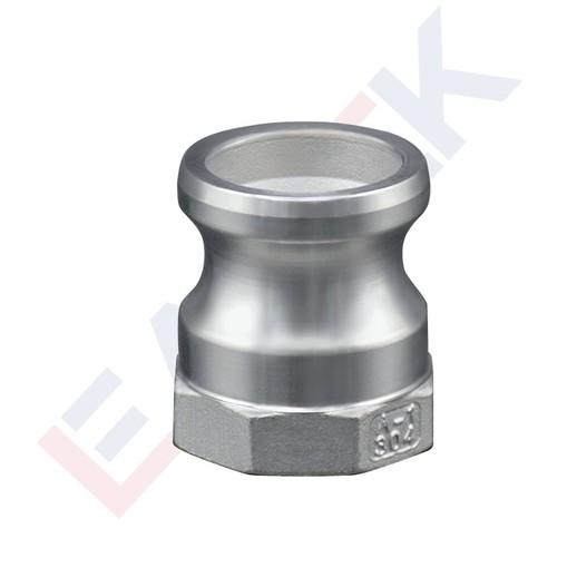
LEADTEK Camlock A
Preventing Particle Entrapment and Shear Shock in Valves
Fittings establish the framework of the pipeline, but valves handle the dynamic work of throttling, isolating, and directing flow. Standard industrial valves are a major source of yield loss because their internal cavities allow particles to settle. CMP slurries, which contain suspended abrasive particles like silica or alumina, are particularly prone to dropping out of suspension when flow velocity decreases inside a valve body. When the valve actuates, these packed sediments are compressed, sheared, and flushed into the process tool as large agglomerates that scratch the wafer surface.
To eliminate these dead zones, high-purity process lines utilize electropolished Sanitary Valves in critical flow loops. These valves are built with zero-internal-cavity designs and ultra-smooth interior surfaces to ensure that fluid velocity remains constant throughout the valve body.
The mirror finish removes the microscopic anchor points where bacteria, polymers, or slurry particles can stick to the walls. During standard clean-in-place or water-flush cycles, the purging liquid clears the entire internal volume, leaving no residue behind to contaminate the next chemical batch.
Beyond particle control, a valve must operate without disturbing line pressure. During precision etching or chemical vapor deposition, fluid delivery must be smooth and linear. If a valve stem chatters or causes a hydraulic hammer effect upon closing, the resulting pressure wave travels down the line and vibrates the spray nozzles inside the process chamber.
This minor physical vibration disrupts the fluid boundary layer on the spinning wafer, causing uneven film thickness or localized over-etching. Advanced flow control components use balanced internal geometries to distribute fluid pressure evenly, ensuring smooth actuation and stable downstream pressure.
The component matrix below details how selecting the proper hardware format remedies these specific pipeline failure modes.
Table 2: Fluid Component Selection Matrix
| Component Type | Primary Function | Core Benefit | ||
| Camlock Fittings | Rapid, secure plumbing connection |
Prevents fluid stagnation and external leaks |
||
| Sanitary Valves | Ultra-pure flow regulation |
Eliminates internal particle accumulation |
||
Metallurgy and Leach testing as Quality Benchmarks
The chemical compatibility of the system metallurgy is the final defense against trace ionic contamination. Standard grades of stainless steel often contain micro-inclusions of manganese sulfide, carbon, or silicon. When exposed to highly corrosive chemicals like hot phosphoric acid or hydrogen peroxide, these surface inclusions dissolve, exposing the raw grain boundaries of the steel to ongoing chemical attack. This leaching process releases free metal ions directly into the chemical stream, which ruins transistor performance if they reach the silicon surface.
Preventing this form of material degradation requires strict quality control during the casting and machining stages. High-purity components must go through rigorous material verification, including optical emission spectroscopy for alloy composition and ultrasonic testing to catch subsurface voids.
Enforcing these strict manufacturing standards guarantees that the equipment can handle continuous exposure to corrosive media over long lifecycles without shedding metallic ions or contributing to process contamination.
Integrating Fluid Systems into Yield Strategies
Contamination control cannot be handled solely by cleanroom air filtration or tool-level recipe optimization. True defect reduction requires a comprehensive look at the entire fluid delivery network. A single sub-optimized valve or a loose piping joint will negate the work of expensive filtration units downstream.
Upgrading to high-precision connection systems and highly polished flow control components allows wafer fabs to remove the material and mechanical variables that cause wafer defects. Deploying reliable fluid joints alongside specialized valves creates a stable, clean, and repeatable chemical environment. In an industry where a single sub-micron particle can turn a high-margin microchip into scrap, the hardware that carries the fluid is directly tied to the factory's bottom line.